東京都港区  プリント基板設計 PCB設計会社 東和サーキット 営業社員募集中 土日祝休み&賞与年2回(業績条件あり) 年間休日125日・働きやすさ抜群 交通費全額支給&テレワーク制度あり (条件あり) 技術と信頼の架け橋

Your Trusted Partner
for PCB Design

We aim to be a reliable partner by delivering sincere work.

With a solid foundation in reliable operations, we have been assisting customers in creating outstanding products for over 40 years. Through this journey, we have honed our expertise in artwork technology and built a legacy in Minato City, Tokyo. From high-speed, high-density implementation PCB design, including simulation, to development evaluation boards and circuit diagram input support, we are here to support your product development.

NEWSお知らせ

STRENGTH

弊社の強み

東京都港区 プリント基板設計 PCB設計会社 東和サーキット 東京タワー風景画像

45 Years of Experience and Proven Results

Flexible and Adaptable PCB Design

Our knowledge and expertise in PCB design have been passed down through generations, allowing us to take on the challenges of ever-evolving technologies as your trusted partner.

東京都港区 プリント基板設計 PCB設計会社 東和サーキット アナログ設計図面

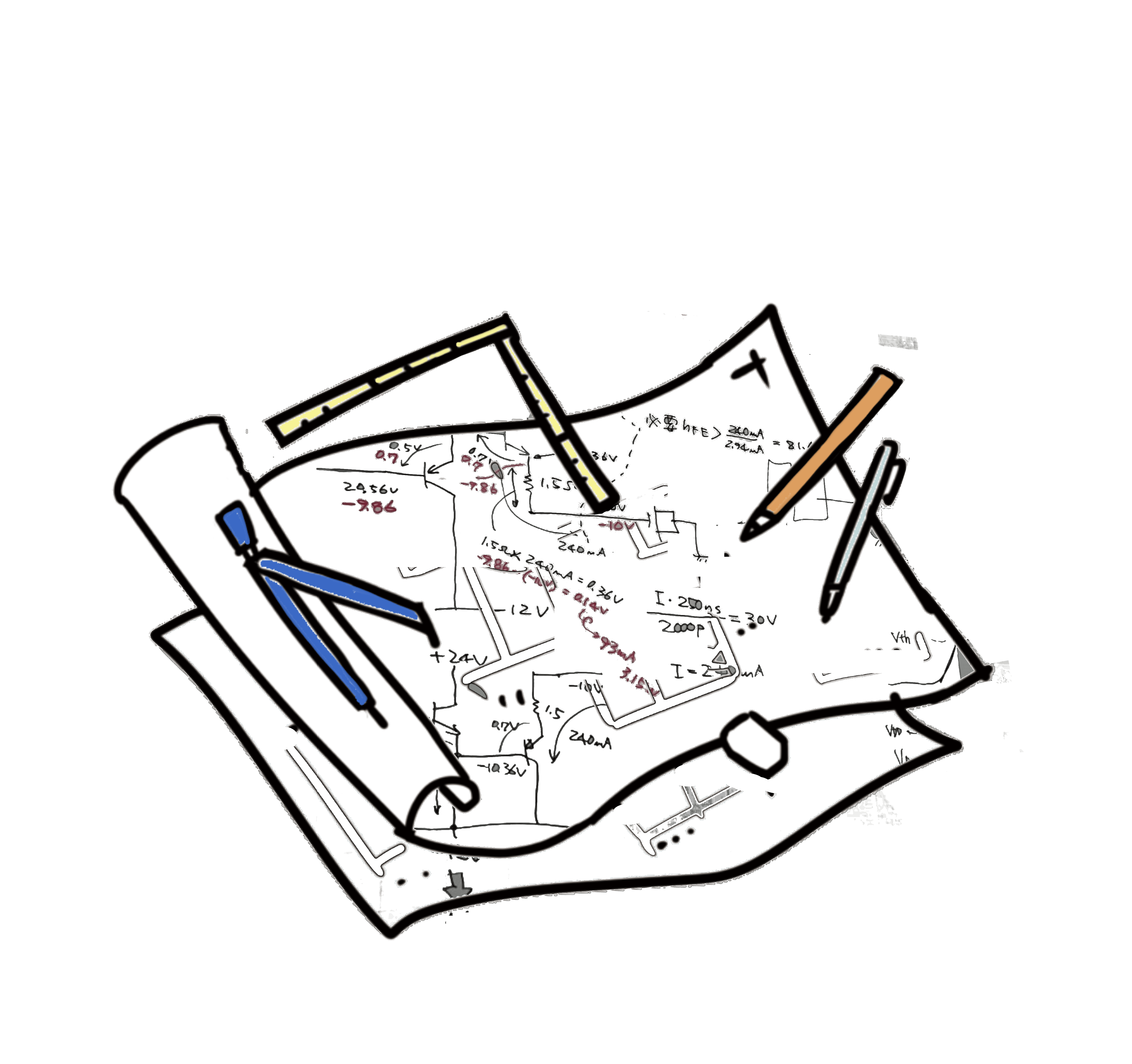
Strong in Analog Circuit Design

Extensive Experience and Accomplishments

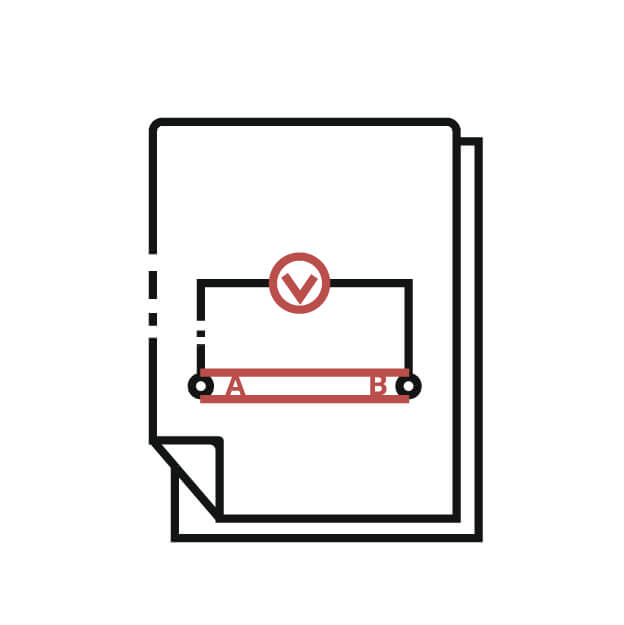
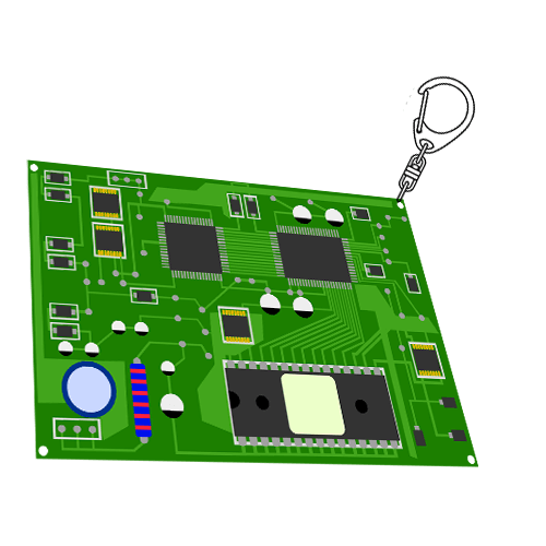
Our company has been designing PCBs since before digital ICs became widespread, boasting over 40 years of experience in analog PCB design. We offer solutions for power supplies, low-frequency circuits, and boards with unique characteristics.

東京都港区 プリント基板設計 PCB設計会社 東和サーキット 回路図面

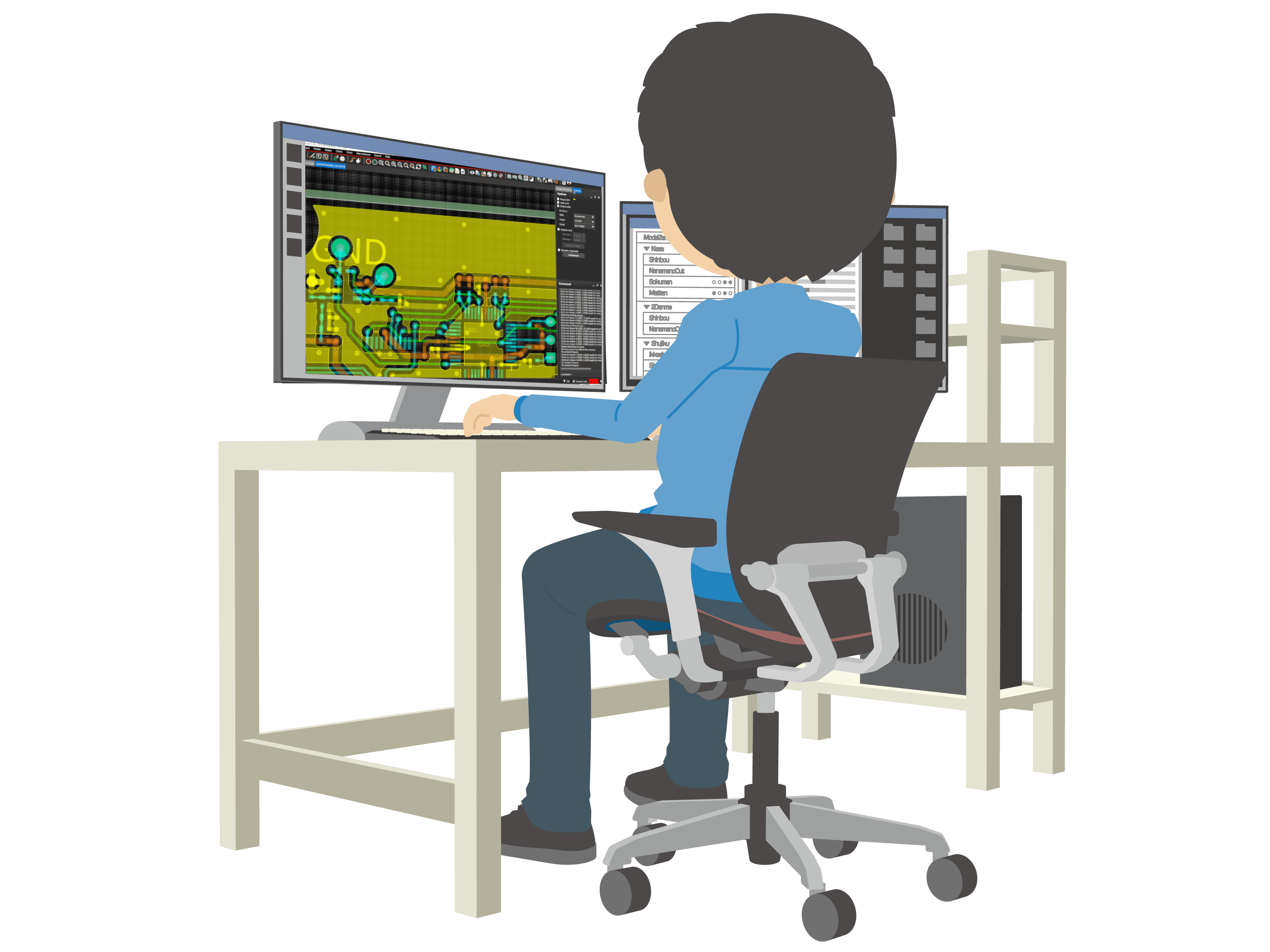
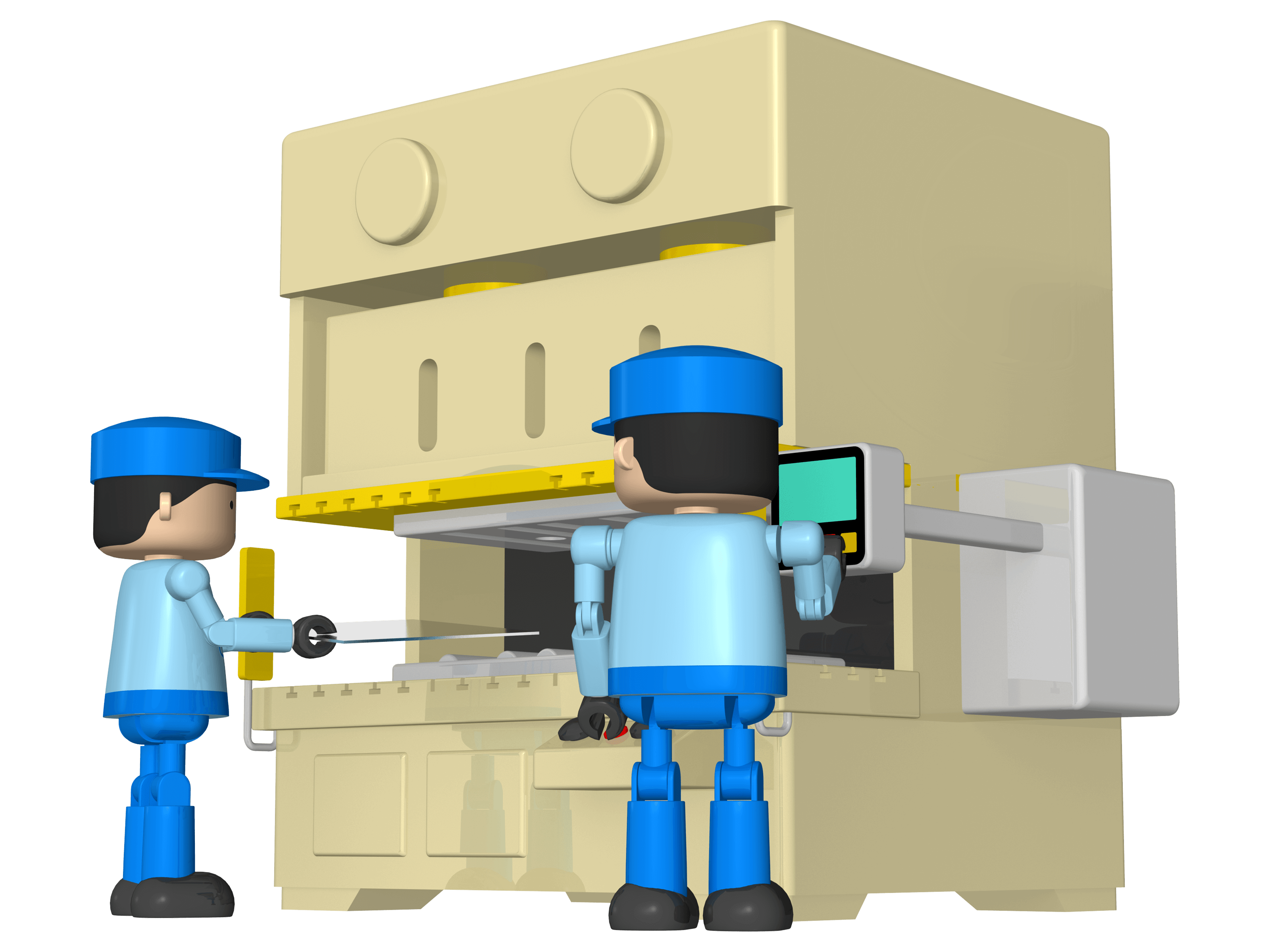
Comprehensive Support

One-Stop Service

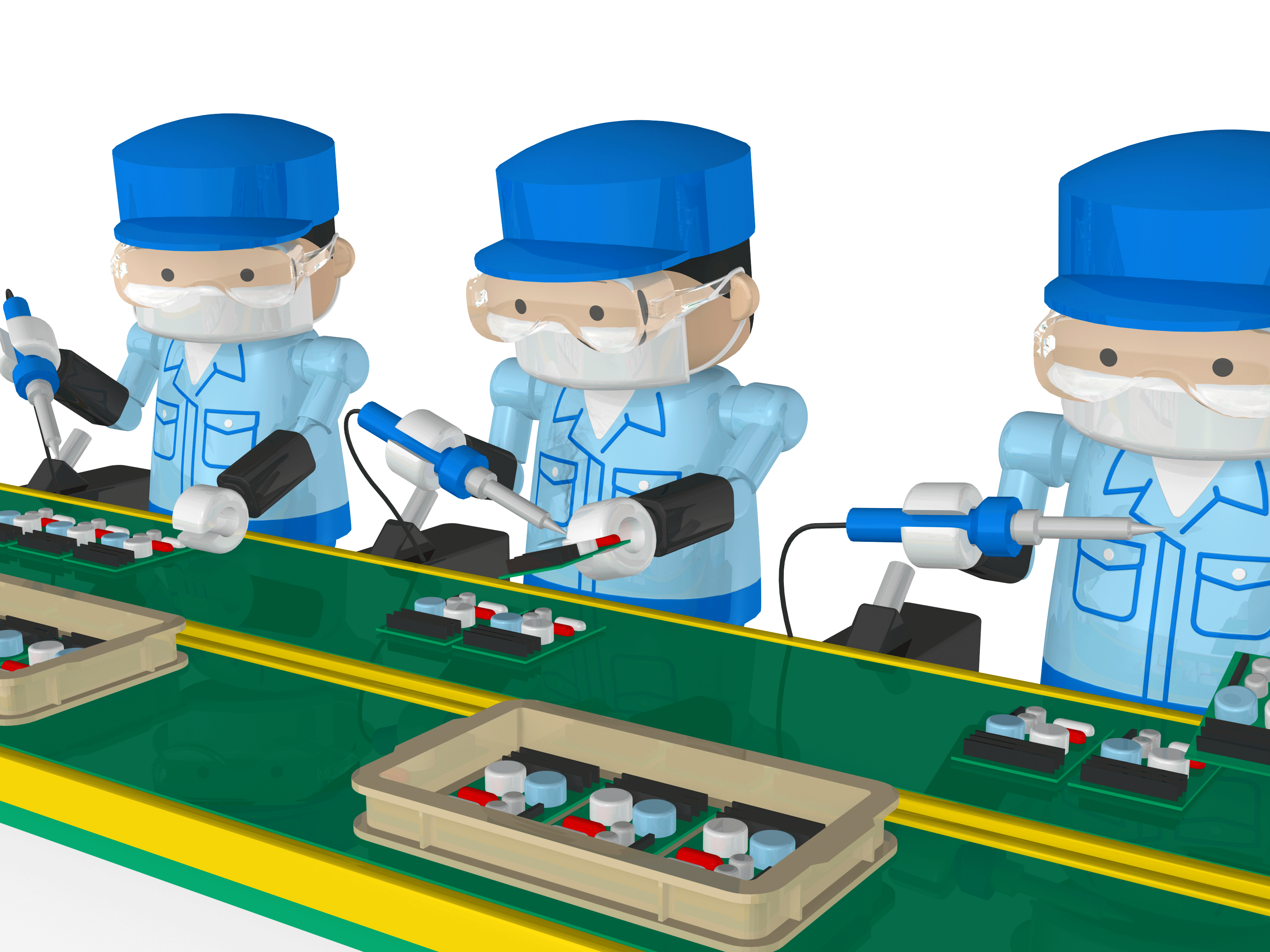
From production management to every step in the process, we offer complete support, including component management, procurement, PCB design, manufacturing, and assembly. We can flexibly adapt to customer needs and provide assistance with assembly, sheet metal procurement, and more.

SERVICE東京都港区 プリント基板設計 PCB設計会社 東和サーキット スマートカー 回路

業務内容

Analog design

Digital design

Circuit design

Board design

Housing design

FLOW

制作までの流れ

東京都港区 プリント基板設計 PCB設計会社 東和サーキット STEP1

Circuit Design
Enclosure Design

東京都港区 PCB設計会社 東和サーキット アナログ設計図面

We design circuits that meet various requirements and function effectively. Simultaneously, we proceed with the design of enclosures that integrate boards and wiring.

東京都港区 プリント基板設計 PCB設計会社 東和サーキット STEP2

Board Design

東京都港区 PCB設計会社 東和サーキット CAD図面パソコン操作

We design boards considering circuit functionality, performance, signal transmission speed, heat dissipation, signal noise, and enclosure constraints.

東京都港区 プリント基板設計 PCB設計会社 東和サーキット STEP3

Board Manufacturing

東京都港区 PCB設計会社 東和サーキット 工場にて機械で製造

We manufacture boards tailored to meet customer needs, including issuing necessary certifications and UL compliance.

東京都港区 プリント基板設計 PCB設計会社 東和サーキット STEP4

Component Mounting

東京都港区 PCB設計会社 東和サーキット コテや機械を使って部品を実装

From 0403 chip components to radial components manually mounted, we handle all types of components and match the quality standards required by our customers.

RESOLUTION

Feel free to discuss these ideas and more!

東京都港区 プリント基板設計 PCB設計会社 東和サーキット 私たちにすべてお任せください!!
東京都港区 プリント基板設計 PCB設計会社 東和サーキット 簡単な設計書があればOK!

A simple design sheet
is enough!

東京都港区 プリント基板設計 PCB設計会社 東和サーキット 光るキーホルダーを作りたい!

Want to create
a glowing keychain

東京都港区 プリント基板設計 PCB設計会社 東和サーキット 動くロボットを作りたい

Want to build
a moving robot?

東京都港区 プリント基板設計 PCB設計会社 東和サーキット ドローンみたいに飛ばしたい!

Want to make something
that flies like a drone

BLOG

東京都港区 プリント基板設計 PCB設計会社 東和サーキット TOWACIRCUITBLOG

We share employee interviews and events happening inside our company!

だるまが導く2025年の挑戦
【2025年スタート!】チームで築くしなやかな未来へ!!

新しい一年が始まり、皆さまいかがお過ごしでしょうか? 先日、厚木市内で行われた「[...]

東京都港区 PCB設計会社 東和サーキット 年末特別号
とわっぴぃがお届けする年末特別号🎉

こんにちは!とわっぴぃです✨ 今年もあっという間に過ぎちゃったね。 みんな、どん[...]

クリアランスと沿面距離の確保
Designing Noise-Resistant PCBs: Ensuring Clearance and Creepage Distances~〜クリアランスと沿面距離の確保〜

Hello, everyone! In this article, we’ll [...]

東京都港区 プリント基板設計 PCB設計会社 東和サーキット 東京働き方改革 東京都港区 プリント基板設計 CB設計会社 東和サーキット タバコルール宣言 東京都港区 プリント基板設計 PCB設計会社 東和サーキット テレワーク東京ルール 東京都港区 プリント基板設計 PCB設計会社 東和サーキット 頑張る女性応援宣言
MAIN CLIANT

主要取引先

東京都港区 プリント基板設計 PCB設計会社 東和サーキット マスコット