
Designing Noise-Resistant PCBs: Ensuring Clearance and Creepage Distances~〜クリアランスと沿面距離の確保〜BLOG
Designing Noise-Resistant PCBs: Ensuring Clearance and Creepage Distances~〜クリアランスと沿面距離の確保〜

Hello, everyone!
In this article, we’ll discuss key points for designing noise-resistant PCBs by focusing on clearance and creepage distances.
In PCB design, clearance and creepage distances are crucial for noise countermeasures and enhancing reliability. Maintaining proper spacing between signal traces and components, as well as ensuring adequate insulation distances along the surface of the board, are fundamental measures to prevent electrical interference and crosstalk.
which are fundamental aspects of robust PCB design.
Let’s aim for even more reliable product designs by mastering these points. In this discussion, I’ll provide practical advice and specific design examples, so be sure to read until the end!

Today, we’ll focus on ensuring clearance and creepage distances as part of the following four strategies:
Utilization of Ground Planes
Separation of Ground and Signal Layers
Ensuring Clearance and
Creepage Distances
Selecting Appropriate Insulation Materials
Now, let’s dive deeper into clearance and creepage distances!
Ensuring Clearance and Creepage Distances
Placement of High-Voltage Components
High-voltage components should be positioned at a sufficient distance from other components and conductive parts of the board to reduce the risk of discharge. Carefully arranging components to maintain clearance improves safety and reliability.
Optimizing PCB Layout
Optimizing the layout involves proper placement of signal and power lines. Sensitive circuits should be separated from high-voltage lines, with adequate shielding and ground placement implemented.
Considering Environmental Factors
Environmental factors like temperature, humidity, and contaminants significantly affect electrical properties. For example, in high-humidity environments, wider creepage distances are necessary, and material selection should account for specific environmental conditions.
Towa Circuit’s Practices for Ensuring
Clearance and Creepage Distances
How Towa Circuit Defines Minimum Creepage Distance
<Internal Standards:>
According to “JPCA_UB01-2021 Version 4: Electronic Circuit Board Standards,” Section 4.6.2-3 states that the minimum conductor spacing depends on agreements between the parties involved. Thus, Towa Circuit regulates minimum creepage distance based on JIS C6950-1:2012, Section 2.10.4.3 (refer to the table for details).
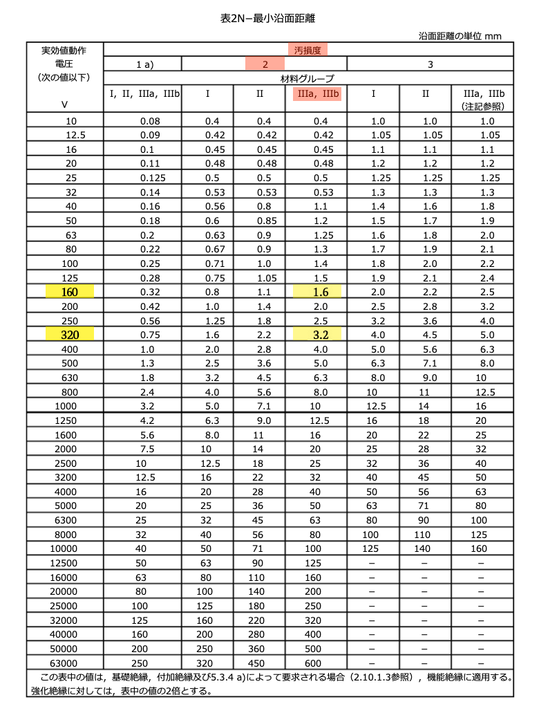
Conditions>> Operating voltage is the RMS value, Pollution Degree 2, Material Group IIIa
Pollution degree classification is specified by the “International Standard IEC60664-1“. In general, this indicates the environment in which the equipment is used.
Pollution Degree 2: Environments where only dry, non-conductive contamination exists ※1 (e.g., offices, labs, homes, control panels)
Pollution Degree 3: Environments with dry, non-conductive contaminants or conductive contaminants such as soil
※2 (e.g., workshops, construction sites)
※1 Generally considered typical use environments.
※2 Listed for reference purposes.
Examples of Material Group and Voltage Calculations
<<Example>>
AC100V RMS value: 100v X √2 = 141.42…v calculated to 160v
AC220V RMS value: 220v X √2 = 311.126…v calculated to 320v
Measures when Creepage Distance Cannot Be Achieved
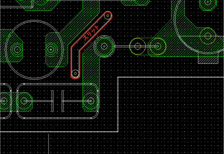
<CASE 1>
When there are space limitations in the component mounting area, such as at the corners of the board, the required spacing cannot be maintained, so a slit is added to resolve the issue.
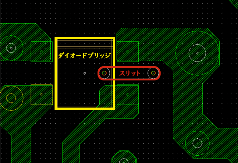
<CASE 2>
At the AC input side of the diode bridge, the pin pitch is fixed, making it impossible to achieve the required spacing. In this case, a slit is added between the pins to create the necessary distance.
<CASE 3>
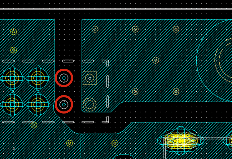
When a blank row is inserted between connector pins but the spacing cannot be achieved, empty pins, which should be through holes, are made into pilot holes to provide the necessary spacing.
Aiming for Highly Reliable Electronic Devices
When it is not possible to achieve the required creepage distance in PCB design, methods such as adding slits or creatively handling empty pins can be employed. This ensures that proper insulation distance is maintained, resulting in a safe and reliable design.
We focus on detailed design solutions to create noise-resistant PCBs.
In the next issue, we will continue to provide valuable information to meet your design needs. We hope you will send us your design requests to help make your projects even more successful.

Next Time…
“Points for Selecting Insulating Materials! The Decisive Factor for Noise Countermeasures”
We’ll be introducing this topic.
Stay tuned~✨

Through Honest Work, We Aim to Be a Trustworthy Partner
For PCB Design, Choose Towa Circuit