
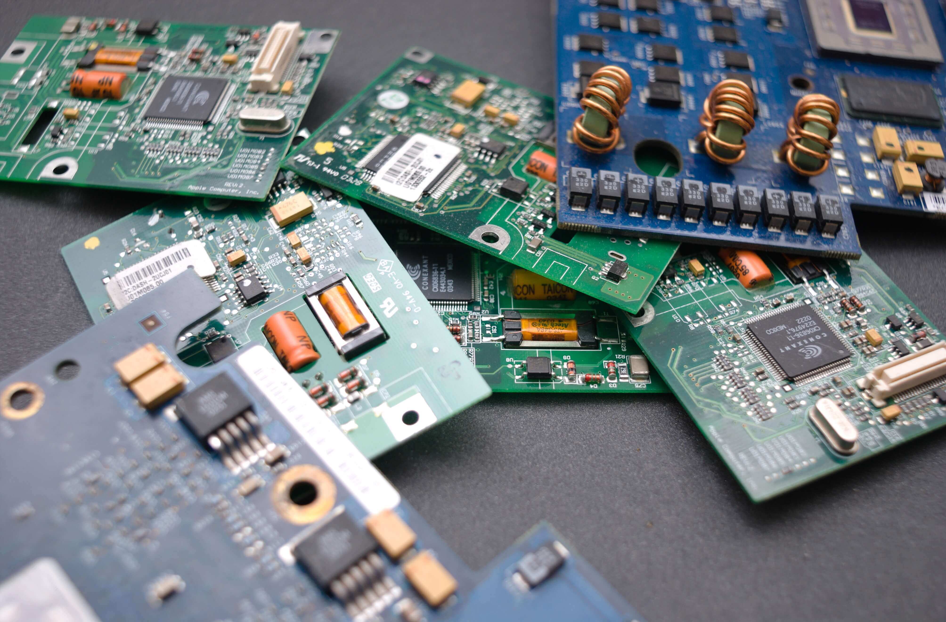
Secrets to Designing Noise-Resistant Printed Circuit Boards~ノイズに強いプリント基板設計の秘訣~BLOG
Secrets to Designing Noise-Resistant Printed Circuit Boards~ノイズに強いプリント基板設計の秘訣~

Hello everyone,
Today, we will discuss key points for designing noise-resistant printed circuit boards (PCBs).
As modern electronic devices become more advanced, noise issues are becoming increasingly complex.
For designers, noise countermeasures are a critical challenge that cannot be ignored.
In this article, we will explore specific techniques to achieve noise-resistant PCB design in detail.
Please read to the end to ensure your product’s reliability.

To design a noise-resistant PCB, consider the following key points:
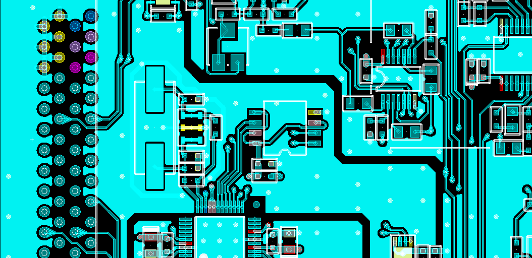
1. Effective Use of the Ground Plane
The ground plane is a large copper layer on the PCB that serves as the circuit’s reference voltage (0V). Understanding its role and placing it appropriately is crucial for reducing noise and improving signal quality.
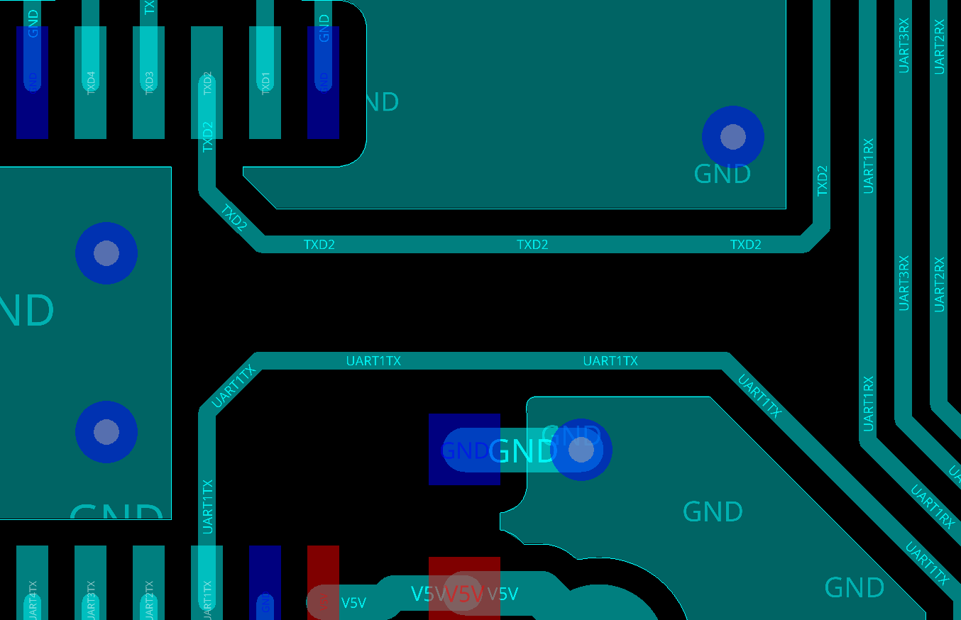
2. Separation of Ground and Signal
Separating the ground (GND) and signal lines on the PCB properly helps minimize noise interference and improves overall performance.
3. Ensuring Clearance and Creepage Distance
Clearance refers to the shortest air distance between conductors of different voltage levels, ensuring electrical insulation and preventing short circuits.
Creepage distance is the shortest path along an insulating surface between conductors. This is particularly important in high-voltage or high-humidity environments, preventing electrical discharge along the surface and improving circuit reliability.

4. Selection of Appropriate Insulation Materials
PCB insulation materials do more than just provide electrical isolation between signals. They also have thermal and mechanical properties that help suppress noise. Choosing the right insulation material improves circuit performance, reliability, and minimizes noise impact.
To design a noise-resistant PCB, it is essential to focus on several key design aspects. Let’s start by looking at the effective use of the ground plane.

Effective Use of the Ground Plane
Ensure a Large, Continuous Ground Plane
The ground plane should be as large and continuous as possible. A fragmented ground plane is less effective at absorbing noise.
Utilizing Multiple Ground Planes
For multilayer PCBs, using multiple ground planes helps prevent interference between different circuit blocks. Connecting these planes with vias ensures consistency and further reduces noise.
Proper Placement of Through-Holes and Vias
When routing signals between different ground plane layers, proper placement of through-holes and vias helps maintain an effective signal return path.

Key Points Practiced by
Towa Circuit in Utilizing Ground Planes!
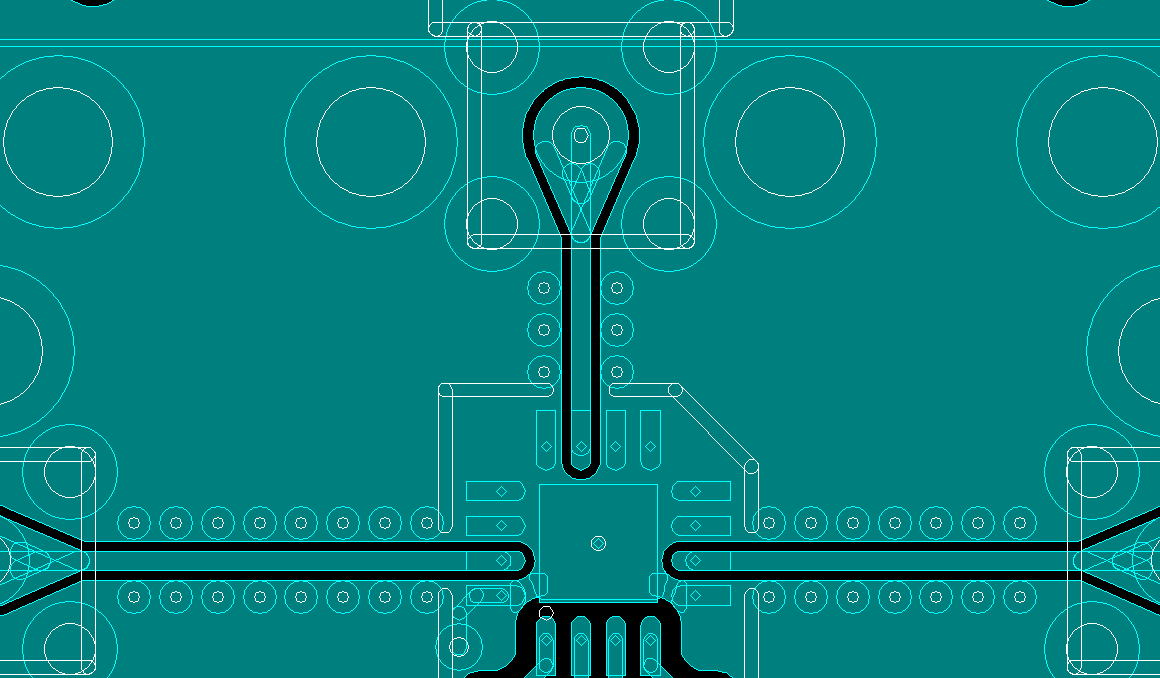
Countermeasures for Antenna Sections on Solid GND
① Cut the Antenna Section
・This cut improves the antenna’s radiation efficiency and prevents unnecessary reflections or losses.
・Enhances the antenna’s radiation characteristics, improving communication range and signal strength.
・Reduces impedance changes and losses caused by the solid GND.
② Add VIAs at the Edge of the Antenna Section
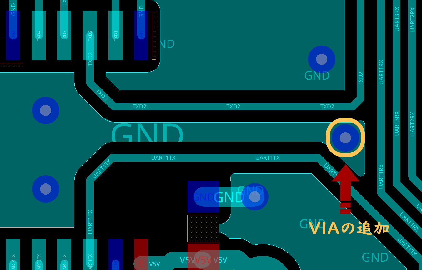
・Adding VIAs improves the overall mechanical strength of the PCB.
・Enhances the electrical characteristics of the antenna, improving signal radiation efficiency.
・Strengthens the ground connection, stabilizing antenna performance.
・Careful consideration during the design phase has a significant impact on the final product’s quality and reliability.
Countermeasures for Antenna Sections on Solid GND
・Reduces noise around the antenna and helps maintain a stable signal.
・The large copper plane effectively shields radiation noise and prevents interference with other circuits.
・Stabilizing the return path improves signal integrity.
・Stable impedance improves signal propagation characteristics.
Aiming for Highly Reliable Electronic Devices
For noise-resistant PCB (Printed Circuit Board) design, several key points are crucial. First, a properly placed ground plane absorbs noise and stabilizes the potential across the PCB.
Next, selecting the right insulation material minimizes signal crosstalk and propagation delay. Ensuring clearance and creepage distances reduces noise impact, while separating ground and signal lines prevents interference between signals.
Additionally, implementing EMC (Electromagnetic Compatibility) measures strengthens the PCB’s resistance to external electromagnetic waves, enhancing reliability. Using noise filters effectively removes high-frequency noise and EMI.
By applying these principles, you can achieve noise-resistant PCB designs, improving the reliability and performance of electronic devices. Addressing these factors at the design stage prevents issues and ensures product quality.
This time, we focused on utilizing ground planes. In the next issue, we will provide a detailed explanation of ground and signal separation.

Next time…
“Ground and Signal Separation”
Stay tuned!✨

We strive to be a trusted partner through sincere work.
For PCB Design, Contact Towa Circuit