
Resonance Analysis for Efficient Product Development~共振解析 製品開発の効率化~BLOG
Resonance Analysis for Efficient Product Development~共振解析 製品開発の効率化~
1. Resonance Analysis for Efficient Product Development
Hello everyone.
Are you utilizing resonance analysis? Reliable PCB design is achieved through the power of resonance analysis.
After PCB design approval, resonance analysis is performed.
Based on the results, problematic areas are identified and improvements are reflected in the PCB design.
Resonance analysis is a crucial step to ensure stability and reliability. By conducting proper resonance analysis, we can improve signal quality and performance while identifying issues in advance.
At Towa Circuit, we accept requests anytime upon customer demand.
※ This is an optional service and requires an additional fee. Please feel free to contact us.

◉ Resonance Analysis After PCB Design
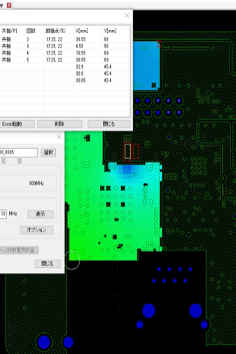
The system used for resonance analysis is DEMITASNX(R) Ver5.1-001.

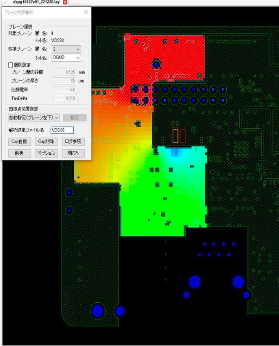
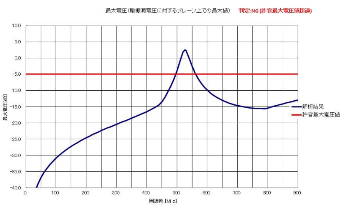
Since resonance components were observed in the power plane relative to the excitation power source, the result was judged as Resonance NG (Not Good).

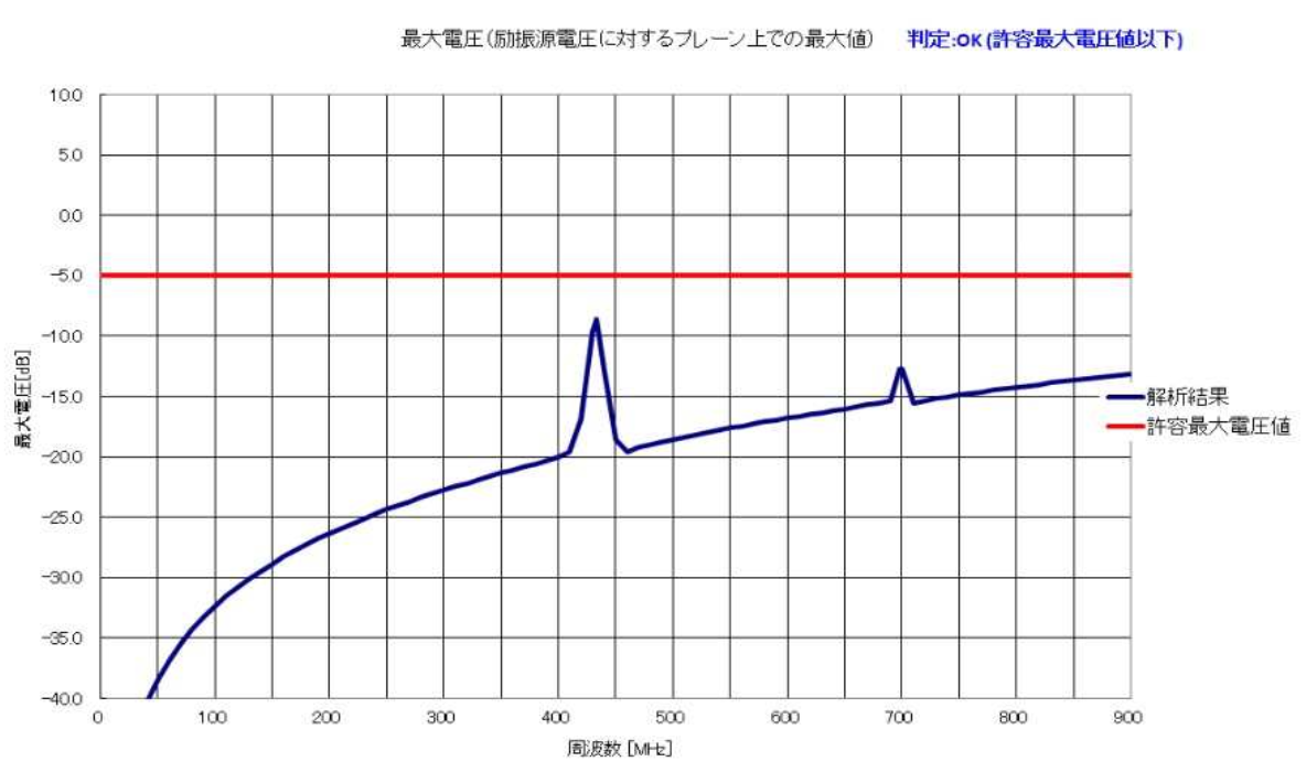
Since no resonance components were observed in the power plane relative to the excitation power source, the result was judged as Resonance OK.
◉ Implementing Countermeasures for Resonance NG Areas
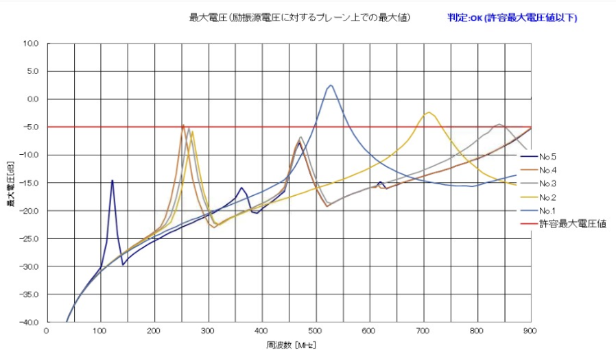
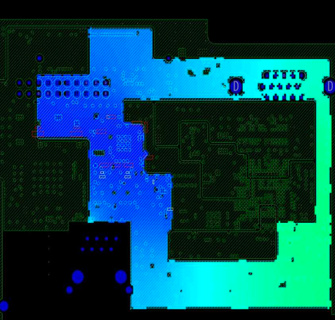
After adding four capacitors in the simulation, the resonance components in the power plane fell below the allowable voltage limit, resulting in a Resonance OK judgment.
—— About DEMITASNX Resonance Analysis ——
【Analysis Result Judgment Criteria】
- 1. No resonance within the analysis frequency range
- 2. Allowable maximum voltage level
- 3. No resonance within the target frequency range: If no plane resonance is detected, it is considered OK regardless of voltage level.
- 4. Allowable maximum voltage: If plane resonance exists, the allowable maximum voltage is applied. If the resonance exceeds the allowable voltage, it is NG; if it remains below the allowable voltage, it is OK.
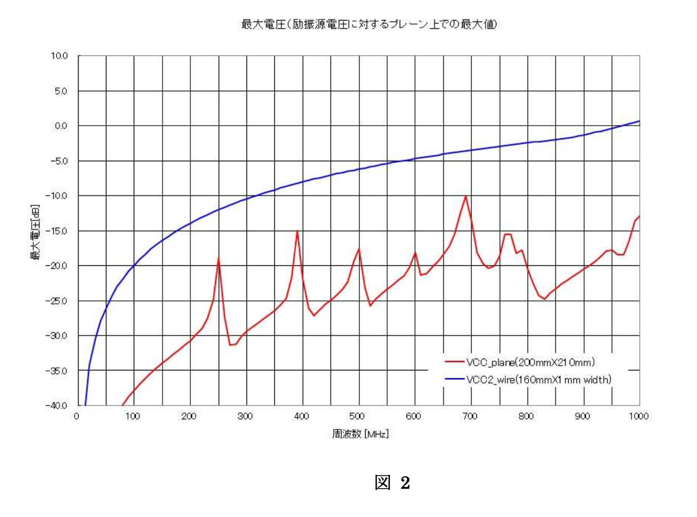
The frequency characteristics graph of plane resonance analysis visualizes the maximum voltage of the target plane at each frequency.
【Plane Resonance and Resonance Analysis with DEMITASNX】
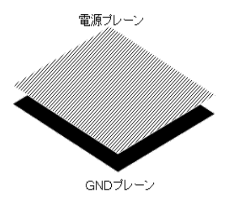
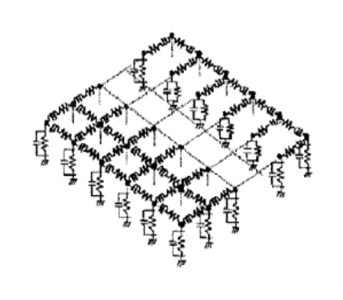
Noise (electromagnetic waves) propagating between the power-ground planes of a printed circuit board undergoes multiple reflections at the plane edges. When the distance between the plane edges corresponds to half the wavelength (or its multiples) at a specific frequency, standing waves form.
This phenomenon is called **plane resonance**, and the specific frequencies where these occur are referred to as **resonance (peak) frequencies**.
The power-ground plane is modeled as an **RLCG equivalent circuit**, and circuit analysis is performed using **SPICE simulations**.
The analysis results are displayed as voltage distribution maps and frequency characteristic graphs.
Relationship Between Allowable Maximum Voltage and No Resonance
When plane resonance is present, the characteristic graph appears as the red line in Figure 2, showing voltage peaks at specific frequencies. On the other hand, when there is no plane resonance, the characteristic graph follows the blue line, indicating an increase in impedance as the frequency increases.
Analyzing the radiated electric field under the same resonance analysis conditions produces the result shown in Figure 3, where the red line indicates a higher radiated electric field.
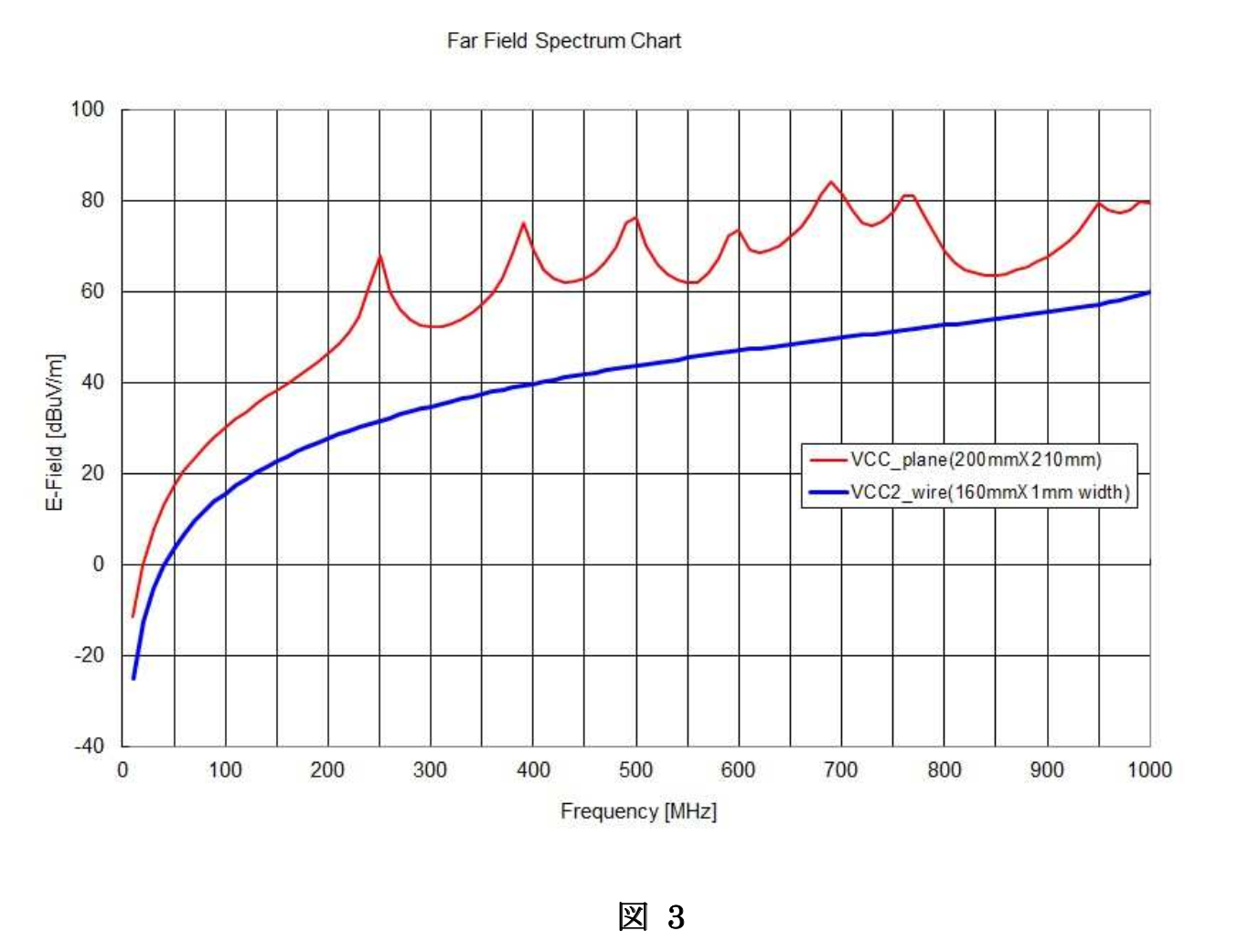
What is Radiated Electric Field?
The far-field radiated electric field is analyzed using the 3-meter method.
The electric field strength (dBuV/m) radiated from the PCB’s power and ground planes at a distance of 3 meters is calculated.
By performing resonance analysis and countermeasures after PCB design,
we provide safer and more reliable PCB operation.

We aim to be a trusted partner through sincere work.
For PCB Design, Choose Towa Circuit