
Evolution to the Next Generation: From 2D to 3D~2Dから3Dへ次世代へ進化~BLOG
Evolution to the Next Generation: From 2D to 3D~2Dから3Dへ次世代へ進化~
Hello everyone,
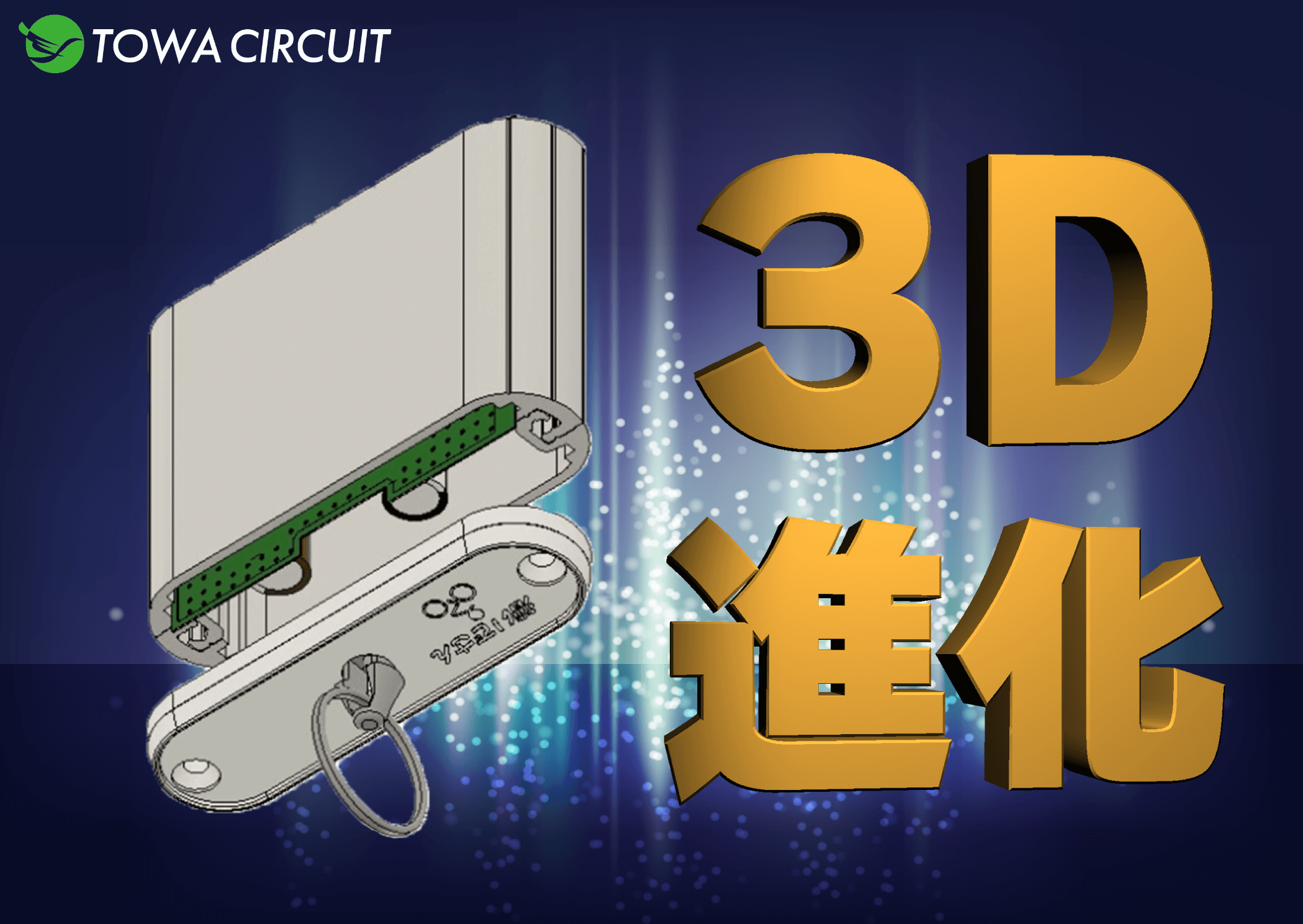
Our technical data is also evolving. PCB design, which was previously limited to 2D data, has now advanced to 3D data thanks to the latest technology. This innovative approach allows for more efficient and precise product realization, from case processing to custom circuit design and PCB layout. By offering PCB design in 3D, we can respond quickly to customer needs and support the development of more advanced products. The video is now available, so please take a look!
▼▼ Click to watch on YouTube ▼▼
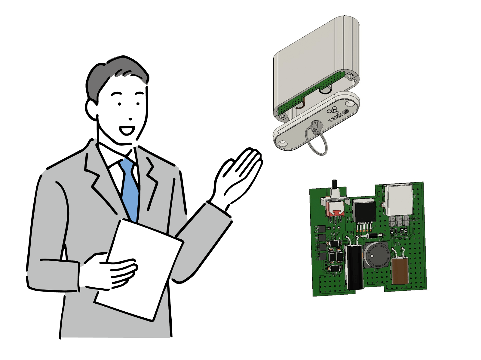
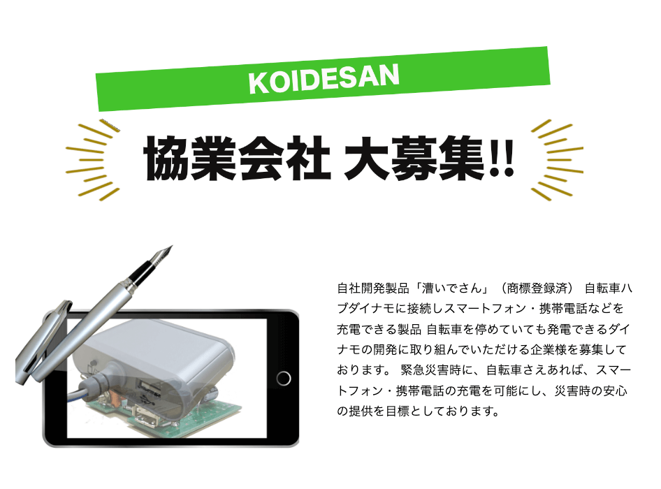
The data shown in the video is from our in-house developed product, “Koide-san” (trademark registered).
The available 3D data formats are STL and STP.
▶︎ For more details, please contact us here ◀︎


Detailed Layout Verification
By using 3D data, it is possible to precisely check the positional relationships of components on the PCB, as well as details such as the thickness and height of the wiring. This helps prevent design issues and errors, ultimately improving the quality of the PCB.

Early Collision Detection
Using 3D data allows for early detection of component and wiring collisions or interferences. This helps to avoid design conflicts and enhances both the productivity and reliability of the final product.
Improved Presentation and Communication
With 3D PCB design data, it becomes easier to visually explain designs to clients and team members. This reduces misunderstandings in communication and facilitates more efficient decision-making.
3D data, with these advantages, plays an essential role in visual information sharing and efficient project management.
We aim to be a trusted partner through sincere work.
For PCB Design, Contact Towa Circuit