
Noise-Resistant PCB Design – Ground and Signal Separation〜グランドとシグナルの分離編〜BLOG
Noise-Resistant PCB Design – Ground and Signal Separation〜グランドとシグナルの分離編〜

Hello everyone,
This time, we will discuss key points for
“Noise-Resistant PCB Design – Ground and Signal Separation.”
Modern electronic devices are becoming increasingly high-performance, and with that, noise issues are also becoming more complex. For designers, noise countermeasures are a critical issue that cannot be ignored.
In particular, minimizing the effects of electromagnetic interference (EMI) is crucial. EMI occurs when external electromagnetic waves negatively impact the operation of electronic devices, directly affecting product reliability and performance.
Noise countermeasures are essential to creating highly reliable PCB products.
In this newsletter, we will explain ground and signal separation in detail. Proper separation of ground and signal helps prevent noise interference between signals and enhances the overall noise resistance of the PCB.
As a result, electronic device reliability and performance are significantly improved.
We will explain specific methods and practical points, so please read until the end. Addressing these issues during the design phase helps prevent problems and ensures product quality.
Let’s continue exploring key noise countermeasures for PCBs.

Four key points for designing noise-resistant PCBs
This time, we introduce ground and signal separation.
Utilizing Ground Planes
Ground and Signal Separation
Ensuring Clearance and Creepage Distance
Proper Selection of Insulation Materials
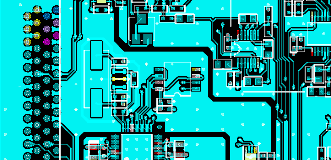
Ground and Signal Separation
Minimizing the Distance Between Signal Lines and the Ground Plane
High-speed signal lines should be placed close to the ground plane to shorten the return path of the signal.
This helps prevent unnecessary noise generation.
Separation of Analog and Digital Circuits
Physically separate analog and digital circuits and use dedicated ground planes for each.
This prevents switching noise from digital circuits from affecting analog circuits.
Placement of Decoupling Capacitors
Decoupling capacitors reduce noise in power lines and stabilize IC operation.
They are especially important for high-speed digital ICs and analog ICs.
Using DEMITASNX is an effective approach for placement.
Utilizing Ground Planes
Key Points Practiced by Towa Circuit!
Connect to the Power Pin through a Capacitor
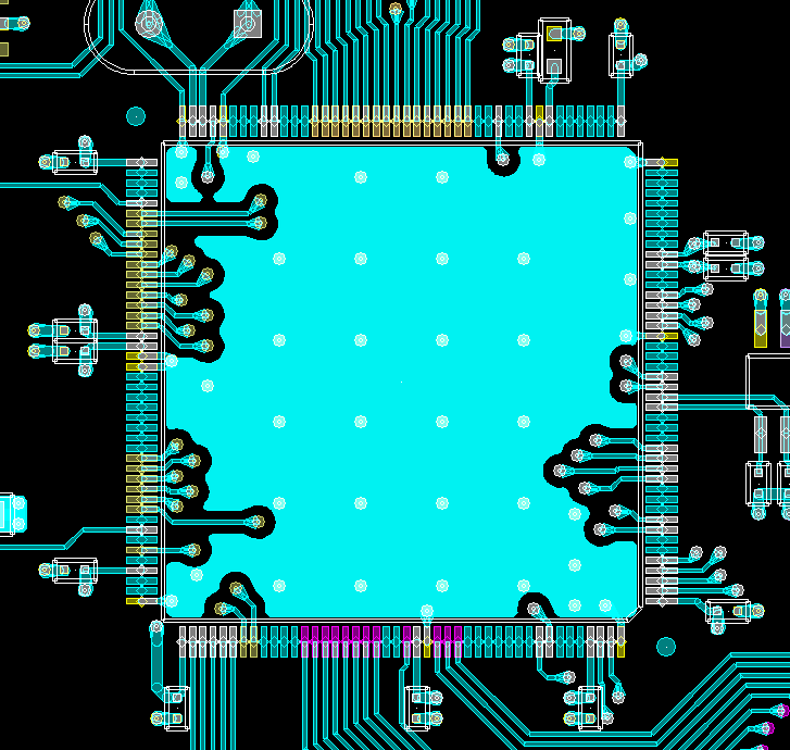
・Decoupling capacitors bypass high-frequency components and prevent noise from affecting the power line and antenna.
・Connecting to the power pin through the capacitor improves the stability of the power line.
・It suppresses voltage fluctuations in the power line, providing stable operating voltage.
Aiming for Highly Reliable Electronic Devices
To prevent noise interference in the power line, it is important to use decoupling capacitors. Decoupling capacitors bypass high-frequency components and prevent noise from traveling through the power line and affecting the antenna.
By connecting to the power pin through the capacitor, the stability of the power line improves, suppressing voltage fluctuations and providing stable operating voltage.
By applying these countermeasures, you can achieve noise-resistant PCB design and significantly enhance the reliability and performance of electronic devices.
Addressing these issues during the design phase helps prevent problems and ensures product quality.
Next time, we will introduce the importance of ensuring clearance and creepage distance.
Stay tuned!

Next Time…
‘Ensuring Clearance and Creepage Distance’
We will introduce it.
Look forward to it~✨

We aim to be a trusted partner through sincere work
For PCB Design, Choose Towa Circuit