Digital Design
digital circuit design
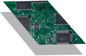
Digital PCB design involves designing circuit boards that process digital signals. Digital signals take on two discrete values, 0 and 1, enabling functions such as MCU control processing and memory control. In PCB design, factors such as signal timing, minimizing the effects of delay noise, appropriate pattern routing, gaps, and guard traces must be carefully considered. To maximize signal accuracy, extracting patterns from the densely packed IC pins and routing requires various design rules and expertise.
What is the Difference Between Analog and Digital Design?
The main difference between analog PCB design and digital PCB design lies in the nature of the signals handled and the approach to the design. In analog PCB design, considerations for voltage and current accuracy, as well as the impact of noise sources, are critical. In digital PCB design, attention to signal timing, shielding against noise, and managing voltage drops are essential.
| Analog Design |
Digital Design |
| Several rooms in a spacious area |
Several rooms in multiple layers |
| Design like the flow of a river |
Design in a square matrix |
| Directly handles voltage and current values of signals |
Handles digitized signals |
| The hands move continuously, representing smooth changes in time |
Changes are represented by a combination of binary data (0 and 1) |